We Can Figure This Out.org
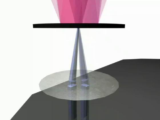
Virtual Lab: Projection Electron Lithography (SCALPEL)
University of Virginia
             
 
© 2003-Present, John C. Bean
 
A step and scan approach is used to print parts of a pattern.

The individual parts of the pattern are then "stitched" together to form one complete pattern on the silicon wafer.

This process is repeated to print several patterns.

In this way, SCALPEL technology prints circuit patterns having extremely small feature sizes (less than 100 nm) over large wafer areas.

 
Last Scene