 |
© 2003-Present, John C. Bean |
|
| |
|
|
|
|
Microelectronic devices are made by repeating two steps: 1) Depositing a thin uniform layer of material; 2) Then using a photographic process to pattern and remove unwanted areas of that layer.
Layer thickness determines the height of the device, photography determines its length and width. So, to make devices smaller, you can make the layers thinner and/or make the photographic features finer.
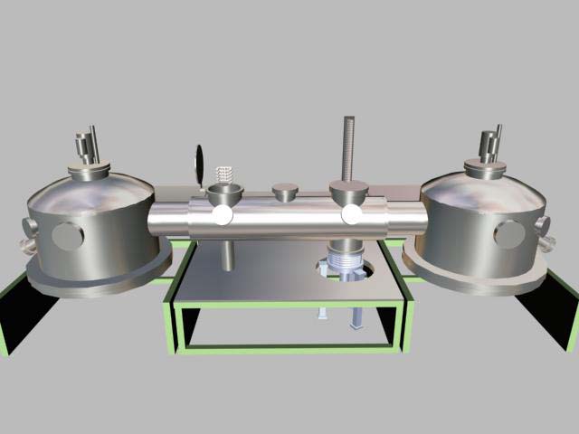
Molecular Beam Epitaxy (MBE) is the all time champ at making thin layers - with MBE one can routinely make layers a single atom thick!
|
|
|
|
|
|
| |
| |
|
|
Next Scene
|
 |
|
|