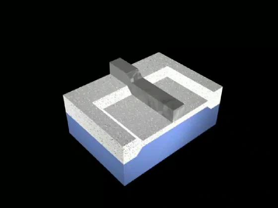
The surrounding SiO2 ring and poly Si stripe are so thick that dopant ions cannot penetrate and reach substrate.
Ions can penetrate thin SiO2 regions.
Where they reach the substrate, they liberate electrical carriers forming the "source" and "drain" regions of the transistor.
These doped regions are automatically aligned immediately to sides of the poly Si "gate."